

TRUMPF has introduced a high-power impulse magnetron sputtering approach aimed at one of the manufacturing challenges behind next-generation AI chip packaging: coating millions of microscopic through-glass vias reliably enough for series production.
The company said its HiPIMS technology can help semiconductor manufacturers create more uniform conductive coatings inside deep, narrow holes in glass substrates. Glass is increasingly being examined as a packaging material because it can support dense interconnects and faster, more efficient data transmission within high-performance chip systems.
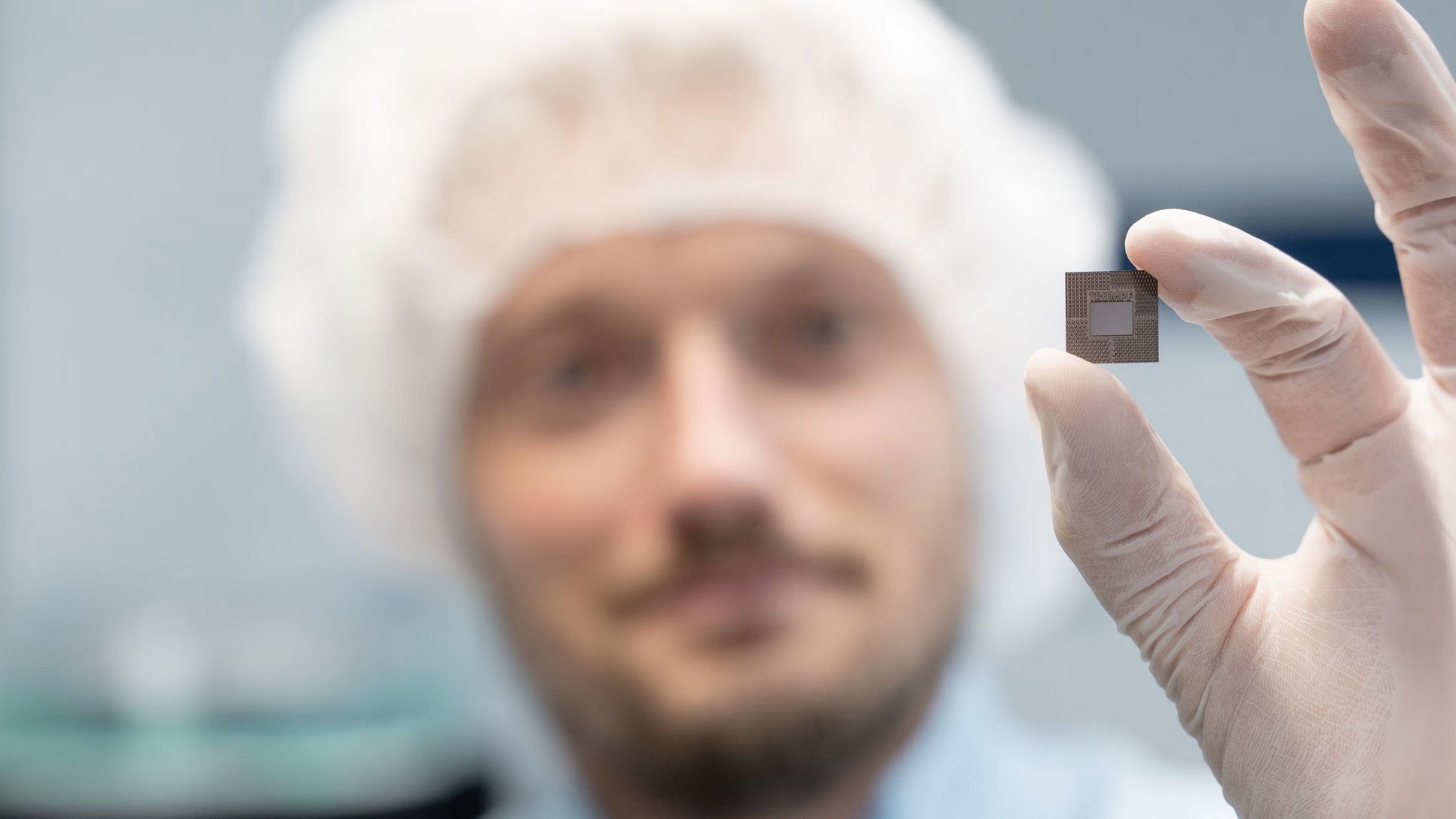
From chip design to packaging
As AI processors pack more computing and memory into constrained physical spaces, performance depends not only on the transistor design but also on the packaging that links chiplets, memory, and other components. Glass substrates are one potential route to denser interconnects, but their production requires holes to be drilled and coated without defects.
TRUMPF said even a small number of poorly coated through-glass vias can make an entire panel unusable. The company is positioning its HiPIMS generators as a way to direct highly ionized particles into those deep structures with greater consistency than conventional coating methods.
The technology uses electric and magnetic fields to guide charged particles into narrow features. According to TRUMPF, the process increases the density of deposited material and can improve coating uniformity in deep trenches. The company did not provide independent yield data or comparative production-cost figures.
A production challenge for advanced packaging
The development matters because new packaging concepts have to clear a difficult industrial hurdle. They must work not only in laboratory demonstrations, but also in high-volume production with predictable yields, repeatable processes, and equipment that can be deployed across multiple facilities.
TRUMPF said it also offers ultrashort-pulse lasers for producing through-glass vias and plasma power supplies for coating and etching in semiconductor manufacturing. Together, those technologies address several stages of advanced packaging, from the creation of the microstructures to their coating.
Demand for advanced packaging is growing alongside AI data-center and high-performance-computing deployments, although the speed at which glass substrates move into mainstream chip production remains uncertain. TRUMPF’s announcement points to a manufacturing constraint that will have to be solved before the technology can support broad commercial volumes.